
As semiconductor device manufacturing gets more and more complex with increased number of steps & smaller critical dimensions of the device, wafer inspection and metrology become more and more critical.
The application requires a dry primary and secondary vacuum system, ensuring efficient and reliable operation. It is designed to maintain low noise and vibration levels, contributing to a quieter working environment. With high performance for high throughput, the system supports fast and effective operations. Additionally, its low power consumption helps reduce operating costs, making it an energy-efficient solution.
CD-SEM
Learn more about CD-SEM
What is CD-SEM?
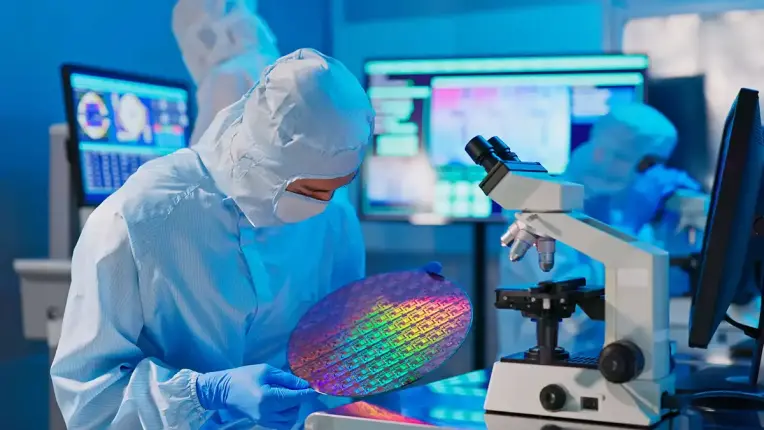
A Critical Dimension Scanning Electron Microscope (CD-SEM) is a specialized electron microscope commonly used in semiconductor production to measure the precise sizes of intricate patterns on semiconductor wafers. It works by directing a focused electron beam over the wafer's surface, capturing detailed images that allow for accurate measurement of important features like line widths and gaps, which are crucial for the performance and yield of semiconductor devices.
How does CD-SEM work?
CD SEM are used to perform dimensional measurements in the range of nm scale, as well as material species analysis. In this type of equipment, the electron beam scans the wafer in a raster pattern. But first, electrons are generated at the top of the column by the electron source and then accelerated and attracted by the positively-charged anode.
The entire electron column needs to be under vacuum. Like all the components of an electron microscope, the electron source is sealed inside a special chamber in order to preserve vacuum and protect it against contamination, vibrations or noise.
Although vacuum protects the electron source from being contaminated, it also allows the user to acquire a high-resolution image. Furthermore, high vacuum increases the collection efficiency of electrons by the detectors that are in the column.
What vacuum conditions are required for CD-SEM?
CD SEM operate under low vacuum, typically in the pressure range of 10-5 to 10-7 hPa (mbar). Because of the low vibration level required, Magnetically levitated turbopump technology is commonly used. Primary vacuum requires low pumping capacity dry pumps to back the turbopumps.
What are the best vacuum solutions for CD-SEM?
Our HiPace Plus turbopump line is the best solution for electron microscopes. The vibration level of the HiPace Plus is significantly lower than standard turbopumps.
As a primary pump, we can offer various dry solutions: Diaphragm MVP series, Multi-stage Roots pumps ACP Series and our newly developed HiScroll series. We can also provide a wide range of gauges for a total vacuum solution.