Please update your browser. It looks like you are using an old version of the Microsoft Edge browser. To get the best experience with the Pfeiffer website, please update your browser.

Contact Login to portal
Global
pvweb_221_allindustries_1200x675_v02_1_semi_sv

Semiconductor Manufacturing

Pfeiffer Vacuum+Fab Solutions is a complete solution provider for the semiconductor industry.

Our innovative and comprehensive portfolio is used in silicon wafer production, from clean room to basement, to increase yield by avoiding contamination and conserving energy.

Vacuum technology for semiconductor industry

The semiconductor industry drives technological progress, influencing our daily lives through devices such as smartphones and AI. Central to these innovations are microchips – tiny yet incredibly complex components that require highly precise and contamination-free manufacturing environments.

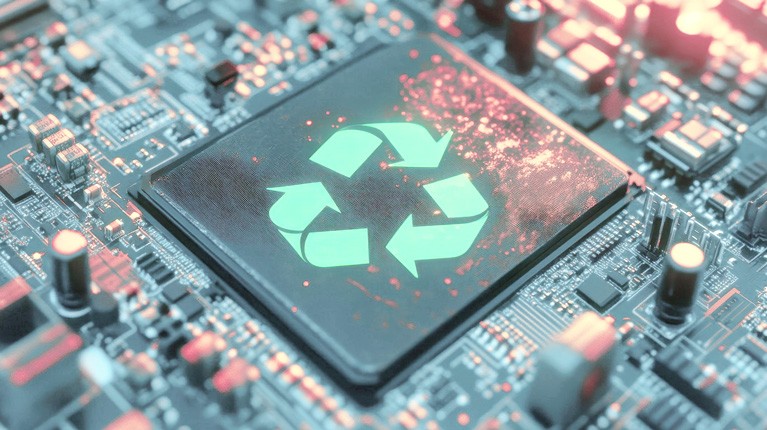
Advanced vacuum technology is crucial to maintaining the contamination-free environments required in semiconductor fabrication.
Semiconductor fabrication is among the fastest-evolving industries, demanding ever higher performance, advanced technology, and sustainability. Advanced vacuum technology is crucial to maintaining the contamination-free environments required.

With nearly 40 years of expertise, Pfeiffer Vacuum+Fab Solutions offers a wide and high-quality portfolio, serving the entire semiconductor manufacturing process – from vacuum chambers to abatement systems. As a one-stop supplier of vacuum and fab solutions, we have a deep understanding of semiconductor industry challenges. Pfeiffer is the right partner to create innovative products that support semiconductor actors in their wafer fabrication challenges. Our role is to connect the dots through product synergies and provide tailored solutions to ensure high yield, reduce energy consumption, and minimize carbon footprint.

Vacuum applications in semiconductor manufacturing

Semiconductor fabs consist of multiple levels, and Pfeiffer products support three key areas to ensure reliable chip manufacturing: At the top, the clean room maintains ultra-low particle levels for wafer processing. Below, the sub-floor hosts utilities essential for clean room function. At the bottom, the basement (sub-fab) houses vacuum pumps, gas treatment, and many more systems crucial for process stability, safety, and environmental control.

Clean room

Semiconductor clean rooms are specialized environments designed to minimize airborne particles, contaminants, and pollutants during the manufacturing process of semiconductor devices. These controlled environments are essential for maintaining the high standards of cleanliness required in semiconductor manufacturing, where even a single microscopic particle can disrupt operations and compromise product quality.

Pfeiffer offers robust turbomelcular vacuum pumps, contamination management systems and valves to meet and maintain optimal pressure and cleanliness required in semiconductor manufacturing. Additionally, our high-performance equipment reduces the total cost of ownership by preventing wafer contamination and adapting to process evolutions.
fab_subfloor_767x767px_1

Sub-floor

Beneath the raised floor of the clean room, the sub-floor houses critical utilities, including air distribution, electrical cabling, and chemical supply lines, ensuring seamless clean room operations.

Pfeiffer was the first supplier to provide point-of-use vacuum pumps qualified by major semiconductor tool makers to ensure vacuum in load lock and transfer tool chambers.

  • Boost productivity with advanced vacuum pump performance for optimized tool operation.
  • Lower total cost of ownership with energy-efficient, low-consumption vacuum pumps.
  • Optimize clean room space with compact point-of-use vacuum pumps.
  • Simplify installation and maintenance with a small footprint and low noise levels.

These solutions help improve efficiency, reduce energy consumption, and support the demanding requirements of semiconductor manufacturing environments.
subfloor

Basement

The sub-fab (basement), located beneath clean room, is composed of one or two basement floors. The basement contains vacuum pumps, abatement systems and exhaust management to maintain process stability, safety, and environmental control.

Pfeiffer offers a comprehensive range of robust and energy-efficient solutions to optimize sub-fab operations:

  • Increase productivity with reliable products and digital monitoring to prevent unexpected breakdowns.
  • Lower total cost of ownership with dry vacuum pumps that consume less power, water, and nitrogen, reducing operating costs and extending maintenance intervals.
  • Support sustainability goals with high-efficiency abatement systems that minimize emissions and environmental impact.
  • Reduce downtime with predictive maintenance solutions and short on-site maintenance activities on abatement systems.
fab_basement_767x767px_1

Semicon services

We are your one-stop shop for cutting-edge semiconductor service solutions.

With our extensive global service and support network, we are always close to our semiconductor customers – no matter where and when.
We deliver the highest quality repair and field service as well as technical support with shortest turnaround times, utilizing a highly-skilled workforce to ensure optimal equipment performance.
  • arpqp_red

    ARPQP

    The new vacuum pump remanufacturing service from Pfeiffer. Especially for the semicon and flat panel market.

    Learn more
  • full_sub_fab_management

    Full sub-fab management

    Holistic on-site service solution for a safe and stable production environment in your semiconductor fab.

    Learn more
  • centrotherm_cs_services

    Gas abatement services

    Comprehensive service packages, following the design and installation of your cleaning system.

    Learn more
  • semicon_service_locations_red

    Semiconductor service locations

    Find your semiconductor service location.

    Learn more

Semiconductor product portfolio

3d_fab

Explore our total fab solutions in 3D

Discover how vacuum solutions from Pfeiffer integrate seamlessly into every stage of semiconductor manufacturing. Navigate our interactive 3D model and see our products in action – from clean room to sub-fab and beyond.

tradeshow_1_thumbnail

00D:00H:00M:00S

Until doors open

2025/09/02 - 2025/09/04

Semicon India

Booth no. 1530

Yashobhoomi (IICC), New Delhi, India

Discover more

Driving sustainability in the semiconductor industry – with Pfeiffer

sustainability_semi
As semiconductor manufacturing evolves, minimizing environmental impact has become a top priority. Pfeiffer Vacuum+Fab solutions drives sustainability with energy-efficient solutions for all vacuum levels that reduce power, water, and nitrogen consumption. Our long-life products further support sustainability by minimizing waste.

Our high-efficiency abatement systems ensure exceptional Destruction and Removal Efficiency (DRE), reducing emissions. Additionally, our manufacturing facilities undergo energy efficiency analyses and operate using renewable energy sources, reinforcing our commitment to a greener industry.

Semicon news from Pfeiffer

Pfeiffer Presents Advanced Vacuum Solutions at SEMICON India 2025

Pfeiffer Presents Advanced Vacuum Solutions at SEMICON India 2025

Pfeiffer Vacuum+Fab Solutions, a member of the global Busch Group, is proud to announce its participation at SEMICON India 2025, taking place from September 2 to 4 at Yashobhoomi (India International Convention Centre) in New Delhi, bringing vacuum and gas abatement technologies to India’s rapidly growing semiconductor sector.

Pfeiffer Vacuum+Fab Solutions at SEMICON Southeast Asia 2025

Pfeiffer Vacuum+Fab Solutions at SEMICON Southeast Asia 2025

Pfeiffer Vacuum+Fab Solutions – a member of the Busch Group and a global leader in vacuum and gas abatement technology – concluded a highly successful showcase at SEMICON Southeast Asia 2025. The event took place from May 20 to 22 and was the first SEMICON Southeast Asia in Singapore since 2013.

Busch Presents Vacuum Solutions for Semiconductor Fabs at SEMICON Korea 2025

Busch Presents Vacuum Solutions for Semiconductor Fabs at SEMICON Korea 2025

The Busch Group presented its comprehensive portfolio for the semiconductor industry at SEMICON Korea 2025.

Showcasing Innovation: Busch Group at SEMICON China 2025

Showcasing Innovation: Busch Group at SEMICON China 2025

The three companies of the Busch Group – Busch Vacuum Solutions, Pfeiffer Vacuum+Fab Solutions and centrotherm clean solutions – will present their extensive range of vacuum solutions jointly at SEMICON China 2025.

Pfeiffer Vacuum+Fab Solutions Presents the New HiScroll 46

Pfeiffer Vacuum+Fab Solutions Presents the New HiScroll 46

Pfeiffer Vacuum+Fab Solutions – a member of the global Busch Group – announces the launch of the HiScroll 46, the newest member of its HiScroll series.

Joint Appearance of the Busch Group Companies at Semicon Korea 2025

Joint Appearance of the Busch Group Companies at Semicon Korea 2025

The three companies of the Busch Group – Busch Vacuum Solutions, Pfeiffer Vacuum+Fab Solutions and centrotherm clean solutions – announce their joint presence at Semicon Korea 2025.

Joint Appearance of the Busch Group Companies at Semicon Japan 2024

Joint Appearance of the Busch Group Companies at Semicon Japan 2024

The three companies of the Busch Group – Busch Vacuum Solutions, Pfeiffer Vacuum+Fab Solutions and centrotherm clean solutions – announce their joint presence at Semicon Japan 2024.

FAQ

How does Pfeiffer support wafer manufacturers?

We provide advanced contamination management solutions that enable semiconductor manufacturers to monitor clean room environments in real time. By detecting contaminants early, our solutions help minimize yield loss.

What pump technologies does Pfeiffer offer?

Our range of dry vacuum pumps includes screw vacuum and multi-stage Roots vacuum pumps.

What makes the vacuum environment unique in the semiconductor industry?

In the semiconductor industry, vacuum environments must comply with stringent clean room standards. All components, including vacuum pumps, are required to meet highly specific industry regulations.

Why are vacuum pumps in the semiconductor industry so specialized?

Vacuum levels in the semiconductor industry must be precisely selected based on the specific application, tool type, and process recipe. Each deposition and etching process – such as ALD, PECVD, CVD, and PVD – requires a controlled vacuum level and pressure, as well as compatibility with various process gases.

Can Pfeiffer Vacuum+Fab Solutions provide tailor-made vacuum systems?

Yes, Pfeiffer delivers customized vacuum systems tailored to the specific needs of semiconductor manufacturers. We combine a wide portfolio of robust, energy-efficient products with deep technical expertise to design solutions across all vacuum regimes – from atmospheric pressure to ultra-high vacuum.

How do vacuum pumps support silicon wafer production?

Vacuum pumps play a critical role in maintaining the ultra-clean environments required for semiconductor processes such as deposition, etching, PVD, lithography, plasma etching, and ALD. By ensuring stable vacuum conditions, they help prevent particle contamination and enable the high precision needed for wafer manufacturing.

Vacuum is essential across all wafer technologies – from traditional silicon to advanced materials like silicon carbide (SiC) and gallium nitride (GaN).

Is Pfeiffer Vacuum+Fab Solutions the right partner to reduce energy consumption in semiconductor processes?

Yes. We offer a broad range of semiconductor products – such as vacuum pumps and process gas abatement systems – engineered with advanced technologies to minimize energy, nitrogen, and water usage. Our solutions are aligned with the industry’s sustainability goals, helping manufacturers lower their environmental footprint without compromising performance.

Why does Pfeiffer offer dry vacuum pumps with a wide thermal range?

A wide thermal range enables our dry vacuum pumps to effectively handle various process gases – from sensitive precursors at lower temperatures to condensable gases at higher temperatures. This capability helps prevent material buildup inside the vacuum system, ensuring stable operation, enhanced reliability, and extended product lifetime in demanding semiconductor applications.

This thermal flexibility is achieved through specialized components integrated into our products. Please contact us to find the best solution for your specific process requirements.